Emulating the NOR flash with an FPGA in the Triax 405 VA
Emulating the NOR flash with an FPGA in the Triax 405 VA |
|
| By Rasmus Rohde |
This document shows how an FPGA was attached to a Triax 405 VA to replace the onboard S29GL032N NOR flash with the goal on running custom code. The big challenge comes from the fact that the flash is in a Fortified BGA packet making soldering of a replacement device a big challenge.
I will skip the usual warnings and disclaimers and let you do the math yourself, but let me make a few points:
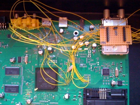
You may wonder why I did not want to attach a flash, mounted in a socket, directly to the PCB, and there are two reasons for this. First of all I did not have a flash programmer and wanted to use what was readily available in my stock. Second I found the task of attaching around 35 wires by hand to an FBGA area to be a very risky task.
The CPU found in the box is an STi7101, which is capable of running in both 8-bit and 16-bit mode. Thus if we make the CPU run in 8-bit mode (16-bit mode is the default in this box), then we can reduce the number of needed data wires from 16 to 8. Already a good start for making the soldering work more manageable. Also the designers of this box were nice enough to place the lower 14 address lines in an area where soldering is much easier than on the actual FBGA pad. The reason these pins are found elsewhere on the PCB is that the boot configuration of the STi7101 is determined by checking whether these pins are pulled up or down.
From the initial observations I decided that mounting 8 data pins on the FBGA area and 8 address pins on the "pull up/down area" would be sufficient to get a usable piece of custom code running. 8 address pins gives us 512 bytes of bootup memory (more on this number later) - hopefully more than enough to kick life into the card reader and bootstrap more code into the system from this peripheral. INSERT PICTURE OF SOLDERED STUFF HERE!
After the soldering was finished I discovered that when the CPU is running in 8-bit mode, A1 is suddenly not the lowest address line, but instead another pin is put to act as A0. Luckily we can use the FPGA to emulate this missing A0 pin and get a free address pin without doing any soldering work. It seems the CPU always reads 32 bits aligned from the flash and by checking the timing of the CPU data access, we can easily recreate A0 by reacting to all transitions of A1 from high to low.
In order to save some soldering work, pins like write enable and chip select were not mounted, and we really do not need these pins as we can just be a little dirty and drive the data bus at all times. Using an external clock to the FPGA (in my case 100 MHz) we can sample the address pins, regenerate A0 and output data on the data bus. Pretty simple.
library IEEE;
use IEEE.STD_LOGIC_1164.ALL;
use work.codemem_package.all;

-- Uncomment the following library declaration if using
-- arithmetic functions with Signed or Unsigned values
use IEEE.NUMERIC_STD.ALL;

-- Uncomment the following library declaration if instantiating
-- any Xilinx primitives in this code.
--library UNISIM;
--use UNISIM.VComponents.all;

entity flash is
   Port ( CLK : in STD_LOGIC;
                         A1 : in  STD_LOGIC_VECTOR (7 downto 0);
          DATA : out  STD_LOGIC_VECTOR (7 downto 0);
          LED : out  STD_LOGIC_VECTOR (3 downto 0);
                         AC1 : out  STD_LOGIC_VECTOR (7 downto 0)
                       );
end flash;

architecture Behavioral of flash is
 signal A1_1 : std_logic;
 signal A2_1 : std_logic;
 signal did_reset : std_logic;
 signal cnt : integer range 0 to 127;
begin

main : process (CLK)
begin
  if(CLK'event and CLK = '1') then
             if (A2_1 = '0') then
                         if (did_reset = '0') then
                           cnt <= 0;
                           did_reset <= '1';
                         else
                           cnt <= cnt + 1;
                         end if;
                       else
                         if(cnt < 100) then
                           cnt <= cnt + 1;
                         end if;
                         did_reset <= '0';
                       end if;

                  if (cnt < 12) then
                    DATA <= codemem_val(A1 & '0');
                         AC1 <= A1(6 downto 0) & '0';
                  elsif (cnt < 25) then
                    DATA <= codemem_val(A1 & '1');
                         AC1 <= A1(6 downto 0) & '1';
                  elsif (cnt < 37) then
                    DATA <= codemem_val(A1 & '0');
                         AC1 <= A1(6 downto 0) & '0';
                       else
                    DATA <= codemem_val(A1 & '1');
                         AC1 <= A1(6 downto 0) & '1';
        end if;

             LED <= A1(6 downto 3);
       end if;
end process;

sample_a1 : process (CLK)
begin
       if rising_edge(clk) then
          A1_1 <= A1(0);
               A2_1 <= A1_1;
       end if;
end process;

end Behavioral;
library IEEE;
use IEEE.STD_LOGIC_1164.all;

package codemem_package is

 function codemem_val(address: std_logic_vector(8 downto 0)) return
std_logic_vector;

end codemem_package;


package body codemem_package is

       function codemem_val(address: std_logic_vector(8 downto 0)) return
std_logic_vector is
               variable data: bit_vector(7 downto 0);
               variable data_stdlogic: std_logic_vector(7 downto 0);
               begin
               case address(7 downto 0) is
       when "00000000" => data := X"36";
       when "00000001" => data := X"d0";

                       when others => data := X"00";

               end case;

               data_stdlogic := to_StdLogicVector(data);
               return data_stdlogic;
       end function codemem_val;

end codemem_package;
The STi7101 includes an SH-4 based CPU and the idea was to make a small bootloader, which will be served from the FPGA emulated flash, and then use the card reader to bootstrap more code. But before getting to all this we need a cross-compiler for the SH-4 platform and to build it, I used buildroot that is an excellent tool for these kind of jobs. With the cross-compiler at hand we are ready to look at the code:
        .text
        .align 1
        .global main
        .type   main, @function

/*
        PIO0_0 = I/OUC
        PIO0_3 = XTALOUT
        PIO0_4 = RSTIN
        PIO0_5 = CMDVCC
*/

main:
        /* Make sure CMDVCC is high and RSTIN */
        mov.l pio0_output_set_addr,r1
        mov  #0x30,r0
        mov.l r0,@r1

        add #0x20,r1
        mov #0x1,r0
        mov.l r0,@r1
        mov #0x31,r0
        mov.l r0,@(0x10,r1)
        mov #0x1,r0
        mov.l r0,@(0x20,r1)

        /* Set CMDVCC low */
        mov.l pio0_output_set_addr,r1
        mov  #0x20,r0
        mov.l r0,@(4,r1)

        mov.l uart_addr,r1
        mov  #0x79,r2
        mov.l r2,@r1
        mov   #0x0,r2
        mov.l r2,@(0x24,r1)
        mov.l uart_control,r2
        mov.l r2,@(0xc,r1)
        mov   #0x0,r0

        /* Set reset low */
        mov.l pio0_output_set_addr,r3
        mov  #0x10,r0
        mov.l r0,@(4,r3)

loop:
        /* Wait for a character */
        mov.l  @(0x14,r1),r0
        and    #1,r0
        cmp/eq #0x0,r0
        bt    loop

        /* Read character */
        mov.l @(8,r1),r2

        /* Wait for room in TX fifo */
        mov.l  @(0x14,r1),r0
        and    #2,r0
        cmp/eq #0x0,r0
        bt    loop

        /* Send byte */
        mov.l r2,@(4,r1)
        bra loop
        nop

sys_cfg7: .long 0xb900111c
uart_control: .long 0x00000589
uart_addr: .long 0xb8030000
pio0_output_set_addr: .long 0xb8020004
        .size   main, .-main
This code is able to read a byte and echo it back. Of course that is not of much use if we want to upload some code. For the full story check out the full 1st stage bootloader.
To generate a useful binary use the following linker script:
SECTIONS
{
  . = 0x0;
  .text : { *(.text) }
  .data : { *(.data) }
  .bss : { *(.bss) }
}
To compile we use sh4-linux-gcc -nostdlib -Wl,-T link.ld bl.o -o bl and to convert this into a flat binary we use sh4-linux-objcopy -O binary bl bl.bin. This can then be converted into the VHDL "case when"-statement by this little piece of C code:
#include <stdio.h>

const char* byte_to_binary(unsigned char x)
{
	int i;
	static char b[8];

	for(i=7; i>=0; i--, x>>=1)
	{
        	b[i] = '0'+ (x&1);
	}

	return b;
}

int main(int argc, char *argv[])
{
	int i = 0;
	unsigned char val[2];

	while(fread(val, 1, 2, stdin) > 0) {
		printf("\twhen \"%8s\" => data := X\"%02x\";\n", byte_to_binary(i++),
                       (unsigned char)(val[0]));
		printf("\twhen \"%8s\" => data := X\"%02x\";\n", byte_to_binary(i++),
                       (unsigned char)(val[1]));
	}

	return 0;
}